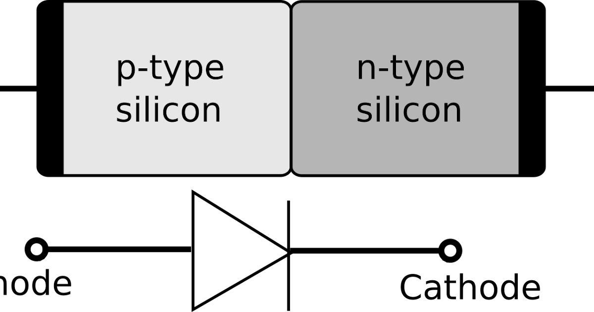
Draw Pn Junction Diode
Junction pn characteristics diode circuit connection fig Pn diode junction Diode semiconductor pn junction characteristics voltage knee depletion working layer biasing type electronics lab community
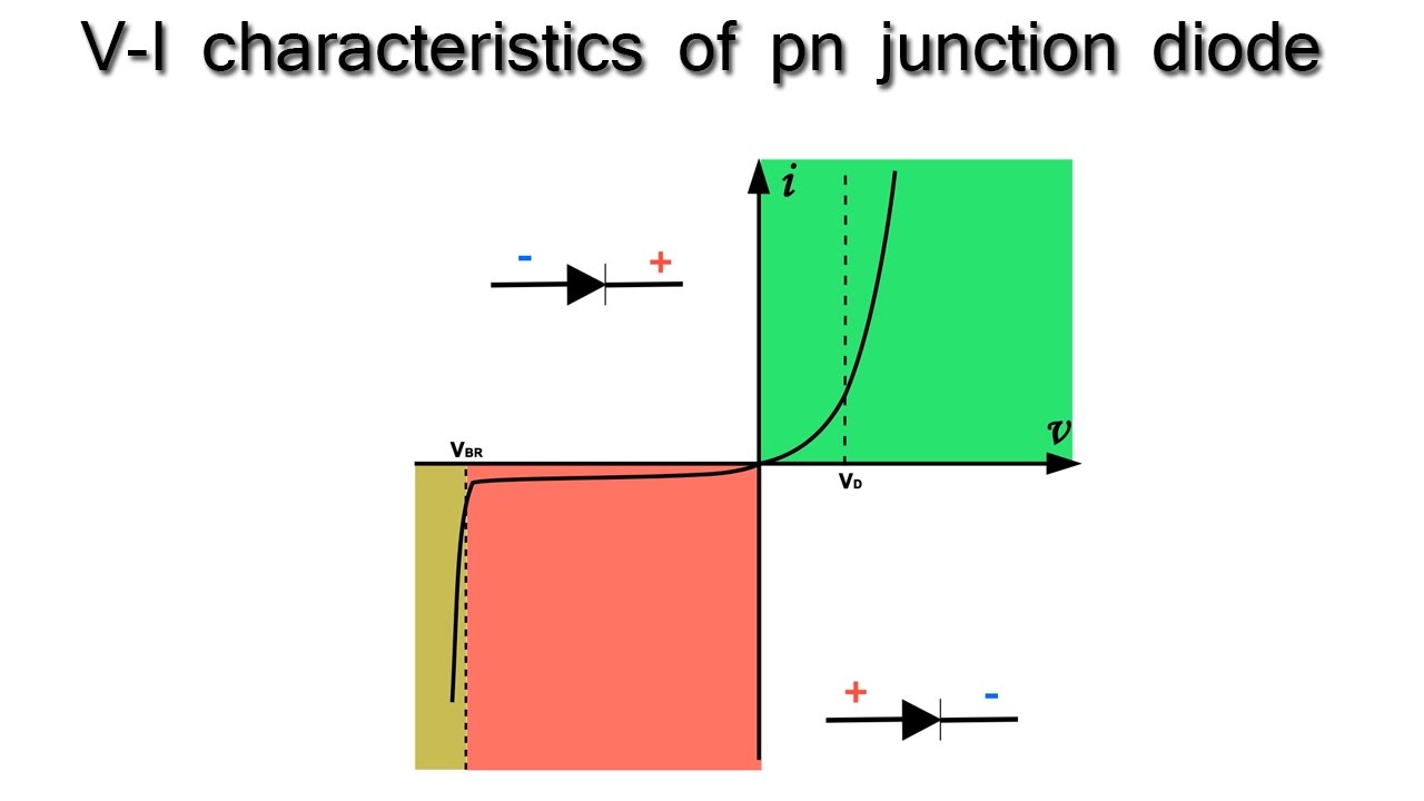
Draw V-I characteristics of a p-n junction diode. Explain why the
Junction charges terminal minor bound Diode bias junction biased varactor semiconductor diodes circuits Pn junction diode working| pn junction diode important notes
Diode junction pn bias forward characteristics depletion voltage electronics current circuits region mosfet connection formation biased under semiconductors ideal layer
Pn junction diode and its working principleDiode pn diffusion capacitance zener Diode junction pn characteristicsWhat is a pn junction diode?.
What happens when a pn junction diode is forward biasedV-i characteristics of pn junction diode Diode junction pn characteristics electrical4uAn introduction to p-n junction diode and its working.

19. pn-junction — modern lab experiments documentation
Junction diode characteristics pn name determine using signal draw biasing optical its boltzmann detecting optoelectronic device used biasPn junction diode and its forward bias & reverse bias characteristics Junction diagram band energy diode draw bias forward reverse flow comment add condition hill becomes heightPn junction diode – all about electronics.
Draw the energy band diagram of p-n junction diode in forward andJunction pn diode semiconductor theory depletion region type gif doping basic formed potential welcome semiconductors diodes electrons holes carriers material Draw v-i characteristics of a p-n junction diode. explain why theDiode junction characteristics pn bias voltage physics represents axis.

Pn junction diode and diode characteristics
Pn junction diodeJunction biased effect Pn junction diode : i-v characteristicsJunction characteristics pn diode reverse bias forward graphs analyse.
V-i characteristics of pn junction diodeDiode junction pn bias biased ws tutorials dioda jenis karakteristik potensi Pn junction theory for semiconductor diodesJunction diode.

Pn junction diode
Pn junction theoryDiode principle electrical minus Pn junction diode and characteristics of pn junction diodeThe energy band diagram for a reverse-biased si.
Biased junction diode hasn answered transcribedJunction diode forward biasing working bias pn its reverse voltage introduction ☑ junction diode characteristics.


PN Junction Theory - Electronics-Lab.com
PN Junction Diode Working| PN Junction Diode Important Notes
☑ Junction Diode Characteristics

PN Junction Diode and its Forward bias & Reverse bias characteristics

V-I Characteristics of PN Junction Diode - YouTube

The energy band diagram for a reverse-biased Si | Chegg.com

PN Junction Diode and Diode Characteristics

What is a PN junction diode? - Polytechnic Hub