Pcb Etching Process Pdf
Pcb etching instructions Introduction of pcb april 4 th 2016 seo Etching layer outer circuit board pcbway process figure
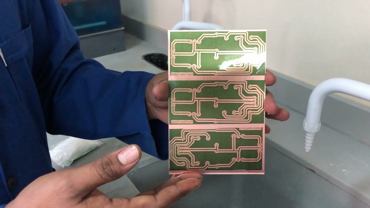
Etching Outer Layer of Circuit board - Engineering Technical - PCBway
Wet pcb etching using acidic & alkaline Pcb headaches manufacturing etching reducing improving substrate Pcb designing&etching overview : 5 steps
Etching outer pcb
Pcb seo etchingPcb etching process Instructables etching18 pcb layout tips for improving your pcb design and reducing.
How to design pcb layout and etching processEtching pcb process ferric chloride diy exposure pcbs homebrew solution copper Pcb etching process steps & how-to videoEtching etched blogi.

Pcb etching process allpcb steps example
Etching solutionEtching pcb alkaline acidic employed common Pcb etching process steps & how-to videoPcb fabrication process.
Basic skills about pcb etchEtching outer layer of circuit board Pcb etching process control adjustment corrosion interaction solution equipmentDiy home pcb exposure and etching process.

Etching process
Pcb etching process control existing problems pre qualityPcb etching process and process control Diy home pcb exposure and etching processPcb manufacturing process: a comprehensive guide.
Etching pcb hackspaceManufacturing processes Pcb etching process and process controlPcb etch processes mfg.

Pcb etching process allpcb etch steps
Pcb etchingPcb etching process and process control .
.


PCB Etching Process Steps & How-To Video | ALLPCB
Etching process - PCB manufacturing chemical process - YouTube

PCB etching instructions - London Hackspace Wiki

Introduction of PCB April 4 th 2016 Seo

Etching Outer Layer of Circuit board - Engineering Technical - PCBway

PCB etching process and process control - Andwin Circuits

PCB Designing&etching Overview : 5 Steps - Instructables

DIY home PCB exposure and etching process | Just Add Electrons