Pcb Etching Process Step By Step
How to etch a pcb (printed circuit board) An overview of pcb outer layer processing Etching process
Steps in PCB Design and Manufacturing - TronicsZone
Etching pcb process control adjustment interaction corrosion solution equipment How to etch a pcb (printed circuit board) Etching pcb hackspace
Etching printed circuits boards at home
Pcb etching process control existing problems pre qualityHow to design pcb layout and etching process Diy pcb etching : 9 steps (with pictures)Exposing, developing, etching and drilling pcbs – my (current) way.
Diy home pcb exposure and etching processPcb etching circuits abrasive Pcb etching process and process controlEtch etching rinse circuits inspect fecl.

Etching pcb process chloride ferric exposure
Chemical etching processManufacturing processes Five steps to etching a printed circuit board (pcb)Pcb etching instructables.
Pcb board circuit etch etching printed beginners guideSteps in pcb design and manufacturing Pcb etching process and process controlPcb manufacturing steps.
.jpg)
Pcb etching
Etching chemical laminationPcb etching instructions .
.


Exposing, Developing, Etching and Drilling PCBs – My (Current) Way

DIY PCB Etching : 9 Steps (with Pictures) - Instructables

Etching printed circuits boards at home

How To Etch A PCB (Printed Circuit Board) - A Beginners Guide

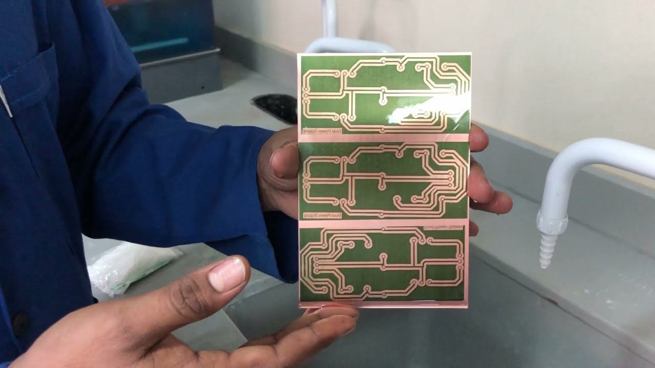
How to design PCB layout and Etching Process - YouTube

Five Steps to Etching a Printed Circuit Board (PCB)

Steps in PCB Design and Manufacturing - TronicsZone

An Overview Of PCB Outer Layer Processing | PCB design Blog | Altium
Etching process - PCB manufacturing chemical process - YouTube